
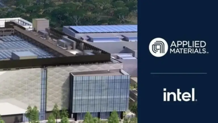
Intel has collaborated with Applied Materials in order to drive future advances when it comes to the chip manufacturing sector.
The companies said the collaboration will include both front-end and back-end-of-line development and that tasks will be done at the R&D campus of Intel located in Hillsboro, Oregon, and Applied’s EPIC – Equipment and Process Innovation and Commercialization Center in Silicon Valley, which is a semiconductor R&D facility scheduled to open later in 2026.
As part of making advancements in the chip manufacturing sector, this collaboration will focus on next-generation transistors and interconnect scaling along with the creation of advanced packaging technologies for Foveros-based 3D stacking to achieve higher interconnect density, better power transfer, and enhanced thermal performance for the high-performance compute platforms that are needed for agentic AI workloads.
According to Dr. Prabu Raja, president of the semiconductor products group at Applied Materials, “With the chipmaking roadmap becoming more complex at each process node, accelerating innovations in semiconductor devices, interconnects, and packaging requires deeper collaboration across R&D and manufacturing. We look forward to working closely with Intel as a founding partner of the EPIC Center to shorten development cycles and bring new technologies to market faster.”
EVP, chief technology and operations officer, and GM of Intel Foundry, Naga Chandrasekaran, added that “accelerating our R&D to keep pace with the rapid buildout of AI infrastructure is critical to delivering the technology, manufacturing excellence, and foundry services our customers expect from Intel Foundry. Applied Materials’ new EPIC Center provides an environment where our teams can collaborate even more closely and at higher velocity to accelerate materials development and process innovations.”
Earlier in 2026, Applied said it would partner with SK Hynix in order to co-develop and co-deploy next-generation DRAM as well as high-bandwidth memory at its $5 billion EPIC R&D facility located in Silicon Valley.