
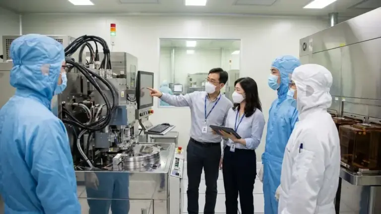
Samsung Electronics on September 11, 2026, announced the outcome of a six-month operational efficiency consulting project at the Nanotechnology Convergence Institute – NINT of POSTECH, which is a member of South Korea’s public nano fab network.
Apparently, the program builds on an agreement signed in March 2025 between the Ministry of Science and ICT as well as three of the leading semiconductor companies from South Korea. Samsung adapted its eye-level consulting methodology, which it traditionally used with suppliers of materials, parts, and equipment, to the public fab environment. Notable achievements include the development of a 5S3Jeong-based field management system, the return of baseline equipment condition, and the institutionalization of preventive maintenance, along with the systemization of standard operating procedures. The government intends to progressively extend this model to all the 14 institutions that are part of the MoaFab platform.
Samsung Electronics has passed on the manufacturing expertise gained within the gamut of semiconductor production to the national public research infrastructure of South Korea. The program is designed to improve the fundamental competitiveness of the domestic semiconductor infrastructure by leveraging private-sector fab management expertise within government-led research facilities.
On September 11, 2026, the Ministry of Science and ICT, along with Samsung Electronics, held a Public Nano Fab Operational Efficiency Consulting Results Presentation at the Nanotechnology Convergence Institute-NINT of POSTECH, announcing the findings of the six-month consulting project.
This project follows an MOU that was signed in March 2025 between the Ministry of Science and ICT along with three big South Korean semiconductor companies—Samsung Electronics, SK Hynix, and DB HiTek.
From March to August 2026, the DS Division Win-Win Cooperation Center of Samsung Electronics sent personnel to NINT to migrate private-sector fab operation and management systems.
The consulting engagement required a complete revamp of fab operations. Samsung put into place the Materials-Parts-Equipment Eye-Level Consulting approach, formerly implemented for semiconductor material, parts, and equipment suppliers, to the attributes of a public fab.
The team went on to identify and reduce potential risks on the shop floor and set up a field management system that was based on 5S3Jeong – Seiri, Seiton, Seiso, Seiketsu, Shitsuke which means organization, orderliness, cleanliness, standardization, and habit formation in addition to correct product, correct quantity, and correct position.
Another key area was equipment reliability. The team brought the operation of the facility within reach of global standards by returning aging equipment to its original operating condition and institutionalizing preventive maintenance procedures. The improvements were codified in standard operating procedures – SOPs so that they would continue after the consulting engagement was over.
Public nano fabs of South Korea have a dual mission – The first is to support semiconductor R&D at universities and research institutions, and the second is to provide an infrastructure for companies when it comes to materials, parts, and equipment sectors that do not have their own fabs to verify and assess their products when it comes to actual semiconductor processes. More equipment uptime consistency and process dependability directly translate into reduced lead times to get R&D results to industrial application.
Public nano fabs of South Korea are the cornerstone of the K-semiconductor ecosystem wherein domestic materials, parts, and equipment companies create and verify new technologies and products, said the executive vice president and head of Samsung Electronics’ Win-Win Cooperation Center, Ji Hyun-ki.
He added, “We will continue contributing to strengthening the overall competitiveness of South Korea’s semiconductor ecosystem by applying the manufacturing innovation know-how accumulated through supplier consulting to public nano fabs.”
It is worth noting that the government intends to use this case as a model in terms of improving operational capabilities at the public fabs of the country. The consulting will be sequentially conducted for the National Nanofab Center, NINT, Korea Advanced Nano Fab Center, Inter-university Semiconductor Research Center at Seoul National University, Next-Generation Sensor and Semiconductor Institute at Daegu Gyeongbuk Institute of Science and Technology – DGIST, and Materials-Parts-Equipment Technology Center at Electronics and Telecommunications Research Institute – ETRI.
More specifically, the government will share consulting findings and best practices for all 14 institutions participating in MoaFab, which is the public nano-fab linkage and integration platform. The vision is to bring the fab operational capacities that have been isolated in individual institutions to the national level.
This is a good example of a win-win cooperation and creates a virtuous cycle within the semiconductor ecosystem, a Ministry of Science and ICT official who also added that in the future, we will push public-private partnership to a new level.