
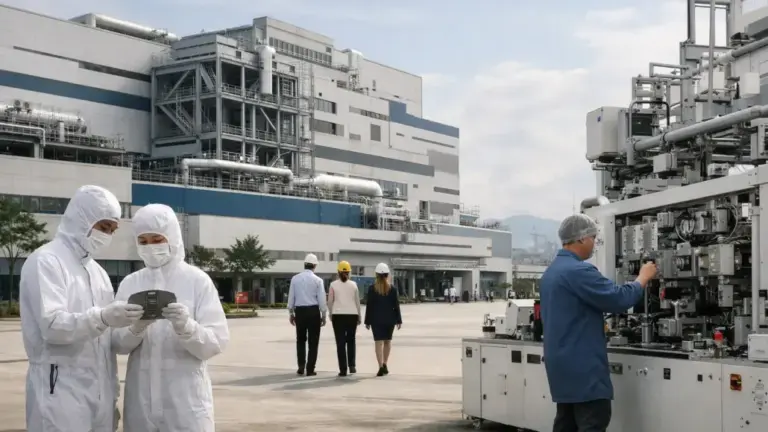
TSMC is growing its presence across the part of southern Taiwan with a new verification line in the Baipu Industrial Park of Kaohsiung, a project with the goal of supporting the development as well as qualification when it comes to advanced semiconductor packaging technologies.
The planned advanced semiconductor packaging plant will enable closer cooperation among chip makers, equipment suppliers as well as materials providers by providing a setting in which technologies can be evaluated and verified before being implemented in large-scale production facilities.
At the latest semiconductor forum hosted by SEMI, TSMC Vice President of Advanced Packaging He Jun said the Baipu site will first cover about 3 hectares and consist of two buildings. The facility will include a modular process verification line so as to support the evaluation of hardware, software, and process integration by suppliers prior to the implementation of technologies within the commercial manufacturing operations.
The project spotlights the increasing significance of advanced packaging in the semiconductor industry. With the rise of demand for advanced applications such as AI, data centers, automotive electronics, and connected devices, chipmakers are concentrating pretty progressively on packaging technologies that allow numerous parts to be integrated into a single system.
Local officials regard the project as a boost to the semiconductor ecosystem of southern Taiwan and a complement to the existing clusters in Nanzih, Renwu as well as Ciaotou. The region aims to develop a more complete supply chain focused on sophisticated semiconductor manufacturing by integrating production, equipment, and materials along with technical service providers.
Suppliers, meanwhile, should view the verification line as a possibility to test equipment and materials in conditions very similar to those encountered in production fab environments. This strategy could help detect integration issues more quickly in the development cycle, decreasing dangers and minimizing the time between developing a product and commercial implementation.
It is worth noting that the advanced semiconductor packaging plant is also anticipated to enhance coordination throughout the semiconductor supply chain. Equipment manufacturers can verify installation and compatibility standards, and materials suppliers may evaluate product performance in a production-like setting. Meanwhile, process engineers can predict potential problems before they impact manufacturing output.
Industry watchers see the project as part of a bigger change in semiconductor strategy. Historically, performance improvement has been driven by advances in transistor scaling, but the growing complexity and expense of cutting-edge process technologies have heightened the importance of advanced packaging, chiplet architectures, and heterogeneous integration.
Thus, competitive advantage increasingly is derived from being able to verify new processes quickly, reduce development risks, and expedite time to production, not just manufacturing capacity. Such validation infrastructure as the Baipu facility is meant to serve those purposes by bringing the development of technology and the performance of manufacturing closer to one another.
The project could also encourage further investment in the semiconductor industry in southern Taiwan. In many cases, closer proximity of suppliers, service providers, and manufacturers in industry groups facilitates collaboration, tackles logistical challenges, and supports quicker problem solving.
The development is a sign of the ongoing evolution of Taiwan’s semiconductor industry beyond wafer fabrication alone. As advanced packaging becomes a key differentiator from AI computation to consumer electronics, facilities that promote process validation and vendor preparedness are likely to grow increasingly crucial to preserving competitiveness throughout the global semiconductor market.