
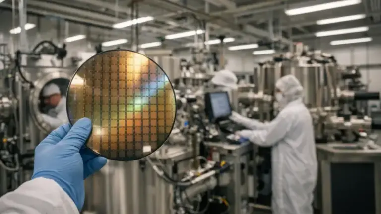
Anderon, which is an IBM company that is dedicated to quantum wafer manufacturing, has gone on to receive a $1 billion award from the U.S. Department of Commerce through the CHIPS and Science Act so as to expedite research and development for its U.S.-based pure-play quantum foundry.
The deal follows a letter of intent that was announced in May 2026 between the Department of Commerce as well as IBM. Anderon is going to make use of the new federal funding so as to expand U.S. quantum wafer manufacturing capabilities and improve access to production-scale technology for companies developing next-generation quantum computing systems.
Anderon has a 300-millimetre quantum wafer foundry in Albany, New York, and has also received an additional $1 billion investment from IBM.
The federal CHIPS award, coupled with IBM’s investment, gives the company a solid foundation when it comes to capital in order to develop domestic quantum manufacturing infrastructure.
Anderon is looking to be a pure-play foundry that serves customers in the larger quantum ecosystem, rather than a vertically integrated quantum computing company that goes ahead and manufactures mostly for its own systems.
The model is meant to provide quantum hardware developers with access to sophisticated fabrication capabilities without the need to build their own semiconductor manufacturing infrastructure.
It is well to be noted that Anderon, at present, manufactures specialized wafers supporting superconducting qubit arrays, quantum input/output signalling and readout signal chain components.
These technologies are essential when it comes to quantum computing systems, forming the basis of the physical building blocks that enable the processing, communication as well as reading of quantum information.
In addition to expanding its U.S. quantum wafer manufacturing capabilities, the company also plans to expand manufacturing capabilities into other quantum modalities over time.
Anderon has already started testing its first quantum wafers via the Albany facility.
The milestone moves the operation out of a strictly research-stage manufacturing environment and shows its capacity to translate pre-production quantum research into manufacturing-grade wafer technology.
That transition could become more relevant as the quantum computing industry shifts to bigger systems and more commercially viable architectures.
The problem with building quantum processors in large numbers is that the materials, fabrication processes and device consistency have to be extremely precise.
To date, many quantum computing companies have relied on research facilities, custom fabrication lines or specialized semiconductor partners to manufacture their devices.
A dedicated foundry model could give the industry more standardised access to sophisticated manufacturing capacity.
Anderson’s Albany facility is based on a 300-millimetre semiconductor manufacturing platform, a format widely used in advanced chip manufacturing, as larger wafers can accommodate more devices per manufacturing run.
The company said its fabrication capabilities are backed by existing quantum intellectual property, a dedicated workforce and billions of dollars in previous investment at the site.
Anderon also provides manufacturing infrastructure to IBM itself, which can support its own quantum computing roadmap.
As IBM moves to more advanced quantum processors and systems, scalable fabrication becomes increasingly important as the company progresses towards larger, more capable quantum machines.
By spinning off the foundry business to Anderon, IBM will be able to maintain access to leading-edge quantum fabrication while also opening up the manufacturing platform to other customers across the industry.
The federal investment also indicates the broadening scope of U.S. semiconductor policy.
While the CHIPS and Science Act has been largely focused on traditional semiconductor manufacturing, advanced packaging and leading-edge logic manufacturing, quantum computers are increasingly being viewed as another strategic technology that must be made onshore.
The $1 billion award places quantum wafer fabrication within the framework of a broader effort to bolster U.S. technology supply chains and reduce reliance on overseas manufacturing infrastructure.
Anderon says scalable quantum manufacturing will be key as the technology moves from lab research towards larger commercial deployments.
Potential quantum applications include advanced materials, chemistry, optimisation and cyber security.
But to scale those applications in a meaningful way, the industry will need to build quantum processors and associated components with much greater consistency and at a much larger scale than today’s research-oriented systems.
Anderon is trying to build the manufacturing base to make that change. The company’s foundry can accelerate innovation by giving customers access to production-scale fabrication while also strengthening domestic supply chains and supporting a broader U.S. quantum ecosystem.
The strategy also mirrors trends observed elsewhere within the semiconductor sector. Pure-play chip foundries have been crucial to enabling semiconductor designers to concentrate on architecture and product development without the burden of owning costly fabrication plants.
Anderon is hoping to replicate a similar model in quantum hardware.
If they are successful, quantum startups and existing tech companies could theoretically design their own processors or subsystems while turning to Anderon for the specialised wafer fabrication they would need to make them.
So the $1 billion CHIPS award is not only an R&D investment but part of a larger effort to build shared infrastructure for the quantum computing industry.
Anderon has ample resources to ramp up capacity, fine-tune manufacturing processes and support customers working across multiple quantum architectures, with IBM contributing another $1 billion and the Albany foundry already processing its first wafers.
According to Mukesh Khare, CEO of Anderon, “This agreement with the Department of Commerce strengthens our ability to deliver the manufacturing scale the quantum industry needs. We’re building a foundation that will let quantum move from research breakthroughs to real-world impact.”
Jay Gambetta, Director of IBM Research and IBM Fellow says that “IBM’s quantum roadmap requires a manufacturing foundation that can scale at the pace our work demands. Anderon’s focus on wafer fabrication gives us exactly that and strengthens our ability to execute and accelerate progress towards the next era of quantum computing.”