
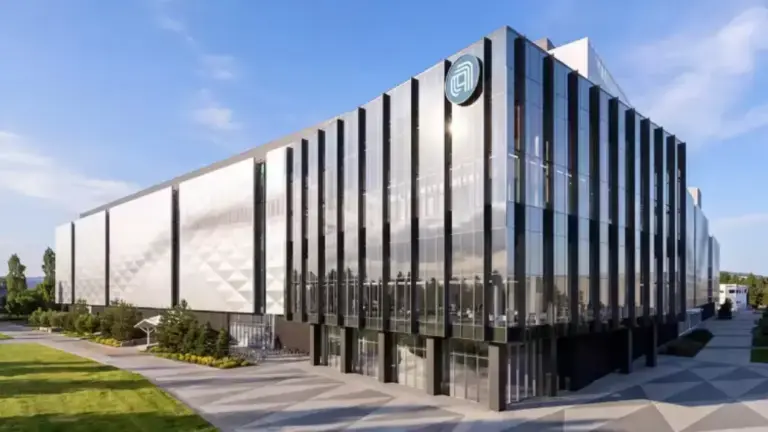
In one of the recent moves that took place in the industry, Applied Materials, Inc., which is the leader when it comes to materials engineering solutions for the semiconductor industry, on October 12, 2026, went ahead and announced the opening of its Equipment and Process Innovation and Commercialization – EPIC Center worth $5bn capital investment in order to create the largest collaborative R&D facility in the world as far as semiconductor process technologies and manufacturing equipment are concerned. It is well to be noted that inside the EPIC Center, top chipmakers, equipment partners, systems companies as well as university researchers are going to team up with the scientists and engineers from Applied so as to accelerate the tempo of chip innovation when it comes to the AI era.
The fact is that as the infrastructure for AI scales, the demands when it comes to high-performance computing are indeed going ahead and creating unprecedented complexity as far as the chipmaking roadmap is concerned, says Gary Dickerson, who is the president and CEO of Applied Materials.
He added that so as to win the race for AI leadership, the industry must rethink as well as re-engineer how they go ahead and work together to design and commercialize the next generation of semiconductor technologies. At EPIC, the leading chipmakers, system designers, and equipment partners, as well as researchers of the world, will be working shoulder to shoulder with the teams to speed the process from breakthrough materials innovation to high-volume manufacturing, which by all means is much faster than ever before.
Designed to Foster Innovation and Commercialization
It is worth noting that the campus of Applied in Sunnyvale, California, on October 12, 2026, unveiled the EPIC Center, which by all means and standards can indeed be regarded as one of the most complex R&D construction projects that exists in the world. The magnitude of its construction can be sought from the fact that the facility itself is 600,000 square feet, with nearly four acres of state-of-the-art cleanroom space, and apparently, it took more than six million construction hours so as to build it. Notably, it has enough concrete in its foundation that can go on to fill 34 Olympic-sized swimming pools and also enough steel in its steel-reinforced structure, which can go ahead and build two Eiffel Towers. Interestingly, 34 roof trusses cover the cleanrooms, and each truss weighs as much as 12 school buses and also stretches nearly 300 feet long.
It goes without saying that EPIC Center worth $5bn capital investment is intended to reimagine the R&D model, which the industry has gone ahead and indeed relied on for decades. In the traditional model, basic materials research is done in one environment, equipment as well as process development in another, and when it comes to process integration and pilot production, it is done in the third, with careful handoff at each and every stage. The EPIC Center aims to eliminate these handoffs by way of co-locating in a state-of-the-art facility that is designed for commercialization for the people who go on to invent the materials, build the equipment, and also make the chips.
Let’s be clear – EPIC is built on a simple belief and which is that the technologies the AI era needs are indeed too complex as well as too important for any single company to go ahead and invent on its own. The EPIC Center launches with a founding roster covering the artificial intelligence – AI technology stack. Founding partners SK Hynix, Micron, TSMC, Intel as well as Samsung Electronics, innovation partners Broadcom, Advantest, and SCREEN, KIOXIA as well as Besi and research partners that include the likes of Stanford University, UC Berkeley, Arizona State University, Rensselaer Polytechnic Institute, and UCLA Samueli School of Engineering.
The fact of the matter is that each partner brings its own set of roadmap challenges and engineers into the facility, thereby working in tight, protected learning cycles with Applied teams. We expect the EPIC ecosystem will continue to attract more companies and organizations over time.
It is worth noting that many of the EPIC Center partner companies were represented by their leaders who attended the unveiling event and got their first look inside the facility. The day started with a summit, which was led by Dr. Prabu Raja, who is the president of the Semiconductor Products Group at Applied Materials, where R&D leaders from top semiconductor design, manufacturing, and equipment companies shared the key challenges facing development and advancement when it came to the global chip industry.
He said that materials innovation is no longer a serial process and that at today’s atomic-scale size, there are many materials and materials interfaces that go on to behave in entirely new ways and that making them work at industry scale requires not just coordinated development but also integrated solutions. He added that EPIC is the only place where they are going to innovate materials and process technology as well as equipment in parallel, which will increase the success rate when it comes to new materials and technologies. Prabhu said that as their customers’ own engineers work to optimize the technology before it gets to their factory, what comes out of EPIC is ready to accelerate to high performance along with high yield much faster.
Interestingly, Applied expects the EPIC operating model to generate a return on both sides of the partnerships. Next-gen materials as well as equipment first go to chipmakers, with shorter learning cycles and a faster route to volume production. Applied gained visibility into many generations of emerging technology issues, determining where the company prioritizes its R&D investments in order to create value for customers and have its services and systems designed in.